
According to recent industry data, the demand for skilled PCB designers with a strong grasp of layout and soldering techniques is on the rise. In order to meet this growing need, it is crucial to understand the intricacies of PCB design, from selecting the right tools and materials to mastering component placement and through-hole technology.
This article aims to provide a comprehensive guide on how to navigate the art of PCB layout and soldering, empowering professionals in this field with the knowledge they need for success.
Key Takeaways
- PCB design software and a multimeter are essential tools for accurate placement and testing of connections.
- Mastering soldering techniques, such as temperature control and proper flux application, is crucial for reliable solder joints.
- Best practices for component placement include grouping similar components together and separating sensitive analog components from noisy digital components.
- Understanding board materials, such as dielectric constant and thermal conductivity, is important for optimal design and performance.
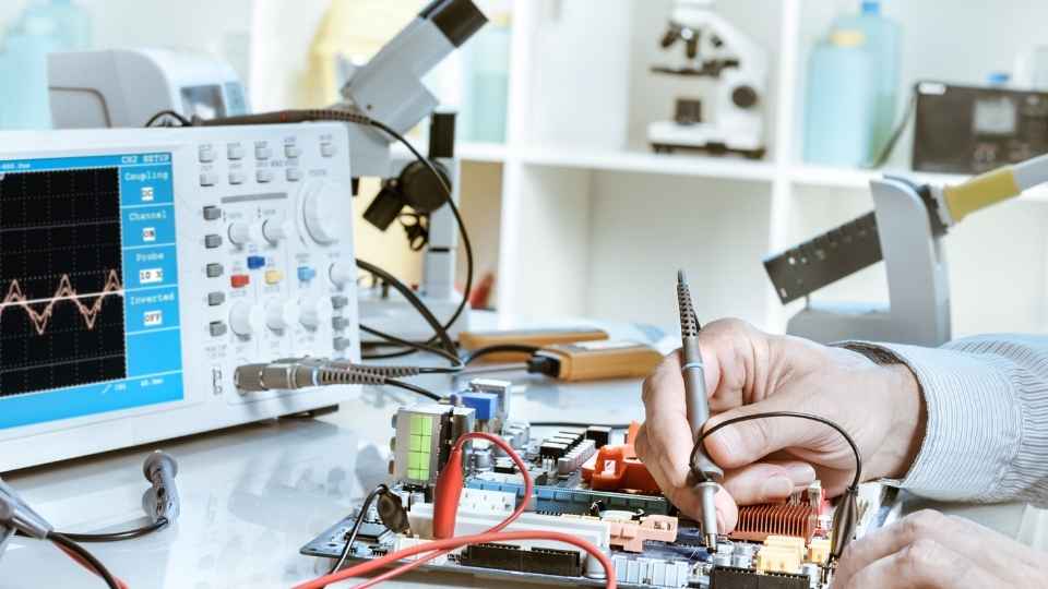
When it comes to mastering the art of layout and soldering in PCB design, having the essential layout tools is crucial for ensuring precision and efficiency. These tools include a PCB design software that allows for accurate placement and routing of components, as well as features like auto-routing and design rule checking to streamline the process.
Additionally, a high-quality multimeter is indispensable for testing connections, measuring voltage levels, and troubleshooting any potential issues. A good quality soldering iron with adjustable temperature control is also essential to achieve reliable solder joints without damaging delicate components.
Other important layout tools include wire cutters, tweezers for handling small components, and a magnifying glass or microscope for detailed inspection.
Mastering these layout tools lays the foundation for successfully mastering the basics of soldering in PCB design.
Mastering the Basics of Soldering
To become proficient in soldering, it is essential to develop a strong foundation by mastering the fundamental techniques and principles. Here are three key aspects to focus on:
Temperature Control: Understanding the temperature requirements for different components is crucial. Maintaining the right temperature ensures proper solder flow and prevents damage to sensitive parts.
Proper Flux Application: Flux helps remove oxidation from surfaces and promotes good solder adhesion. Applying an appropriate amount of flux is vital for achieving reliable solder joints.
Solder Joint Inspection: After soldering, inspecting your work is imperative to ensure quality connections. Look for smooth, shiny joints that are free from cracks or voids, as these indicate a well-executed soldering job.
Best Practices for Component Placement in PCB Design
Proper component placement is crucial in ensuring optimal circuit performance and minimizing signal interference in electronic systems. When designing a printed circuit board (PCB), it is essential to follow best practices for component placement to achieve the desired functionality and reliability.
One important consideration is placing components near their corresponding connectors or ports to minimize trace lengths, reducing the chances of signal degradation or noise pickup.
Additionally, separating sensitive analog components from noisy digital components can help prevent cross-talk and interference. Grouping similar components together, such as resistors or capacitors, can simplify assembly and troubleshooting processes.
Furthermore, considering thermal management by spacing high-power components adequately apart can prevent overheating issues.

Following these guidelines will result in a well-designed PCB that meets the requirements of freedom-seeking individuals who desire reliable and efficient electronic systems.
Understanding Board Materials for Optimal Design
Understanding the properties and characteristics of different board materials is essential for achieving optimal design in electronic systems. Here are three key considerations when selecting board materials:
Dielectric Constant: This determines the speed at which signals propagate through the board and affects signal integrity. Lower dielectric constants are preferable for high-frequency applications.
Thermal Conductivity: Efficient heat dissipation is crucial to prevent component overheating. Materials with higher thermal conductivity help dissipate heat more effectively.
Mechanical Strength: The board material should have sufficient mechanical strength to support components and withstand environmental stressors such as vibrations or shocks.
By carefully considering these factors, designers can select the most appropriate board material that meets their system requirements and ensures reliable performance.
Now, let's explore the value of through-hole technology in PCB design...
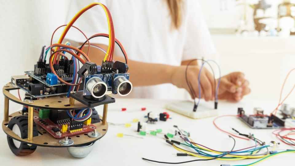
Exploring the Value of Through-Hole Technology
Through-hole technology offers several advantages in electronic system assembly, including enhanced durability and reliability due to the strong mechanical connections it provides.
This method involves inserting component leads through holes in a printed circuit board (PCB) and soldering them onto copper pads on the opposite side. The resulting connection is secure and resistant to vibration or mechanical stress, making it ideal for applications that require robust performance.
Through-hole technology also allows for easier inspection and repair of PCBs, as components can be easily removed or replaced if necessary.
Furthermore, this method is compatible with various types of components, such as resistors, capacitors, and integrated circuits.
While surface mount technology has gained popularity in recent years, through-hole technology remains a valuable option for designers seeking dependable and long-lasting connections in their electronic systems.
Frequently Asked Questions
What Are the Common Challenges Faced When Designing PCB Layouts and How Can They Be Overcome?
Designing PCB layouts can present various challenges, such as signal integrity issues, thermal management, and component placement. These can be overcome through meticulous planning, utilizing design rules and guidelines, conducting thorough simulations, and collaborating with experienced engineers.
Are There Any Specific Soldering Techniques or Tips That Can Help Ensure a Successful Solder Joint?
To ensure successful solder joints, specific techniques and tips can be employed. These include proper heating and cooling cycles, using the right soldering iron temperature, applying flux for better wetting, and ensuring adequate solder coverage on the joint.
The placement of components on a PCB can significantly impact the overall performance and functionality of the circuit. Proper placement ensures signal integrity, minimizes noise, reduces interference, and optimizes thermal management, leading to improved reliability and efficiency of the circuit.
What Are the Different Types of Board Materials Available for PCB Design and How Do They Impact the Design Process?
Different types of board materials, such as FR-4, polyimide, and ceramic, impact the design process in terms of electrical performance, mechanical durability, thermal management, and cost. Careful selection is crucial for optimal PCB design.
What Are the Advantages and Disadvantages of Using Through-Hole Technology in PCB Design Compared to Surface Mount Technology?
Through-hole technology in PCB design offers advantages such as strong mechanical connections, easier repairs, and better heat dissipation. However, it can be more time-consuming and expensive compared to surface mount technology.
 Basic Electronics ConceptsEssential ToolsCircuit Design BasicsMicrocontrollersDIY Electronics ProjectsRoboticsPrivacy PolicyTerms And Conditions